Article Index
1 – Introduction to VRM
Today, a small article about VRMs. I wrote it few months ago further to the overclocking problems encountered by the Radeon HD 5970 (see HERE and HERE) with FurMark.
These overclocking problems have a common source: VRMs. Fundamentally, VRMs are power supply units. The conception of such devices is a difficult work (voltage and current stability, size of heatsinks, OCP (over current protection), etc.) and sometimes some parts may be under-sized. Under-sized VRMs can lead to a malfunction of the card when the current the VRMs have to deliver is too high (due to a high GPU load). Recent cards like Radeon HD 5000 series come with an advanced OCP management (the GPU is throttled back to reduce the current the VRMs have to deliver, see HERE) but on other cards, an over-current may lead to a system reboot (maybe due to the rig PSU OCP too) or even kill the card (see HERE – in that case, the OCP didn’t work at all…). In this article, I’ll try to explain the basic notions about VRMs and where they are located on the PCB (printed circuit board) of a HD 5970.
These principles are more or less the same for all graphics cards (the components can be different but have the same function).
As usual, if you have additional information and resource or if you detect some errors, just drop a comment.
2 – VRM: Theory
The Voltage Regulator Module or VRM is a device that performs DC-DC conversion (DC = Direct Current). This conversion is fundamental because many chips, like the GPU in our case, do not operate at 12V or 5V but at lower voltages like 1V. Then devices to reduce the voltage are required and these devices are the famous VRMs. So a VRM is a DC-DC converter. The other goal of a VRM is to provide a constant DC output voltage as well as providing a lot of current (amperes) to the GPU.
A VRM is also called a buck converter.
Here is the basic scheme of a VRM:
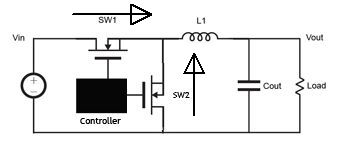
The SW1 is a transistor that commutates the input voltage, L1 is an inductor that stores and releases energy into a capacitor Cout allowing to smooth the voltage signal. SW2 is a freewheeling transistor that is closed when SW1 is opened. In low power buck converters, a diode is used in place of the transistor.
A VRM can be divided in three parts: the logic device, the power device and the filtering device.
The logic device, also called voltage controller, drives the power device in order to supply the GPU with the correct voltage and current. The voltage controller is the brain of VRM.
The power device is the VRM muscles and are made up to power MOSFET (Metal-Oxyd Semiconductor Field Effect Transistor). A MOSFET is power switching element and is one of the most common transistor type in electronics.
The filtering device allows to smooth the MOSFET output current and is made up of inductors and capacitors.
A phase is made up of a power device and a filtering device. The phase allows to simplify the description of a VRM: a VRM is made up of a voltage controller and several phases.
The following images show the VRM of Asus’s EAH 5830 DirectCU:
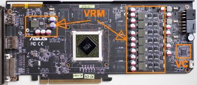
Asus EAH 5830 DirectCU PCB with VRM phases and voltage controller (VC) – source
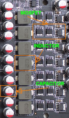
Asus EAH 5830 DirectCU PCB – VRM details
Asus EAH 5830 DirectCU – voltage controller details
According to the global view of the PCB, this Radeon HD 5830 has 8-phase VRM. There are one or two phases for feeding the memory (yes, graphics memory is also fed by the VRM) and the other phases are used to feed the GPU (6 or 7 phases).
Why a VRM is made up of several phases ?
Because modern GPUs require a lot of current: up to 80A for some GPUs. Yes, dear readers, 80 amperes! So much current can only be provided by a VRM with several phases. Such kind of VRM is called a multiphase VRM or multiphase converter. Multiphase can be replaced by n-phase.
Actually all modern graphics cards come with a multiphase VRM.
In a multiphase VRM, each MOSFET (actually there are two MOSFETs per phase) is driven by a PWM signal generated by the voltage controller. The PWM command signal drives the opening and closing of these power MOSFETs.
The output of a n-phase VRM is the sum of each phase.
PWM means Pulse Width Modulation and is simply a signal with a square pulse whose the width can vary.
The following image shows the PWM signals for a 4-phase VRM:
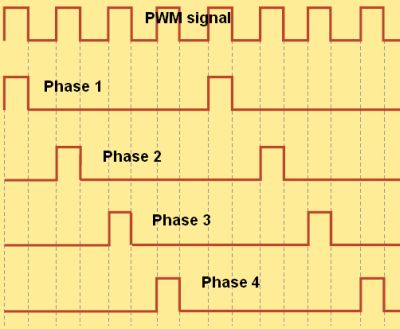
4-phase VRM – PWM signals
The PWM principle is rather simple: the nature does not support brutal variations (of voltage, speed, whatever quantity you want) and prefers smooth ones. Just drop a rectangular pulse wave (the voltage), whose pulse width is modulated, in a filtering device that accepts only smooth signal variation and the result will be an average value of the waveform. And this average value is linked to the pulse width.
In a n-phase VRM, each couple of MOSFET delivers only 1/n of the total output power, allowing smaller MOSFET and inductors. What’s more, the power dissipation is spread over all MOSFETs, avoiding an unique hot spot that exists in a single phase VRM.
There are two kind of PWM generators: analog and digital. Quickly said, analog PWM generators use simple electronic compoments (continuous signal generator, comparator, etc.) to generate the PWM signal.
Digital PWM generators are based on a micro-controller and offer programming capabilities.
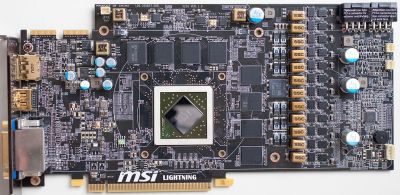
So the amount of power that a VRM can deliver is proportional to the number of phases. MSI has understood this simple principle and has equipped its high-end Radeon HD 5870 Lightning with a 15-phase VRM (12 phases for the GPU and 3 for the memory)!
The filtering device in each phase is actually a way to store (when MOSFETs are closed) and transfert (when MOSFETs are opened) the energy required by the GPU. There two main types of VRMs:
– Inductor-based VRMs
– Capacitor-based VRMs
Capacitor-based VRMs are suitable for handled devices (low power) while inductor-based VRMs are suitable in presence of high current with low voltage. In this case, the inductors are called high current inductors. These high current inductors feature a low inductance (typically 2.0 uH and below) and a high current rating (15A up to 100A).
A choke is the common name given to a power inductor used in a filter element.
Keep in mind that the GPU operates with very low voltage and high current signal (the current per phase can reach 20A or more). In this situation the inductor acts as a reservoir for the current avoiding brutal variations of current (inductors chokes are passive components that are designed to resist changes in current). The inductor stores the energy in the form of a magnetic field. This filter can be also seen as a low-pass filter for the current.
3 – VRM: Radeon HD 5970
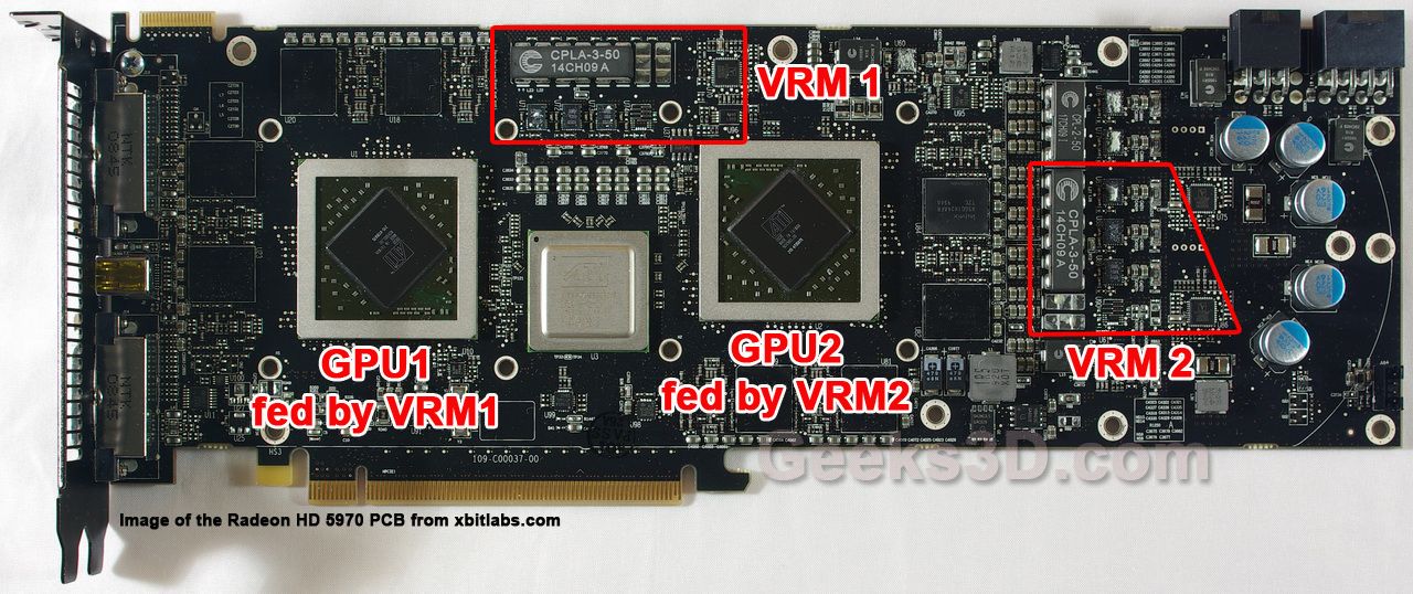
Radeon HD 5970 VRM – Click to enlarge
The Radeon HD 5970 is a dual-GPU graphics card and two VRMs are used to feed both GPUs.
Here is the diagram of a HD 5970 VRM:
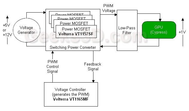
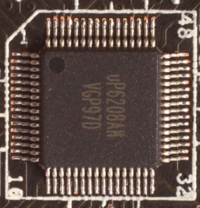
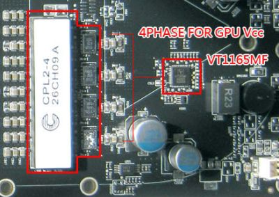
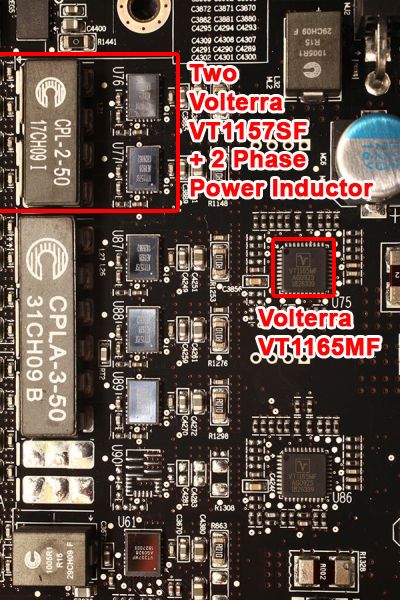
The HD 5970 voltage controller is a Volterra VT1165MF. This component allows to adjust the GPU voltage up to 2.0V (and adjusting the voltage of each GPU separatly is possible in theory…). The default voltage is 1V. The HD 5970 is softmod compatible: the voltage can be changed by software.
The VT1165MF drives three power MOSFETs with a PWM signal. Each power MOSFET is materialized by a Volterra VT1157SF. On a HD 5970, each GPU is fed by a 3-phase VRM.
Each GPU of the Radeon HD 5970 requires less energy than the GPU of a Radeon HD 5870. That’s why there are only 3 phases to feed each GPU (vGPU for GPU voltage) on a Radeon HD 5970 while there are 4 phases on a Radeon HD 5870:
Radeon HD 5870 and the 4-phase VRM (source)
AMD has reserved some place to add another phase on the HD 5970. Ultra high-end Cypress-based cards like the Asus Ares (true dual-HD5870) need 4-phase VRMs per GPU.
These power components dissipate a lot of power that’s why, on modern high end graphics card like the Radeon HD 5970 (of a GTX 480), they are equipped with heatsinks like this Radeon HD 5850:
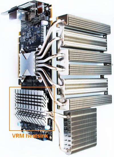
Radeon HD 5850 with Thermalright VRM-R5 heatsink (source)
The VRMs of the Radeon HD 5970 are inductor-based VRMs. This kind of VRM requires off-chip inductors.
These off-chip inductors are materialized by the Coiltronics CPLA-3-50, a 3-phase power inductor (which has been designed exclusively for use with Volterra devices). The CPLA-3-50 is a 3-phase low noise component (yes, the inductor can sometimes generates a buzzing noise depending on the amount of current that is passing through…), each phase offering an inductance of 50nH (nano-Henry).
If you discover the term of Henry for first time, just know that the Henry is the unity that allows to describe an inductor. A capacitor is described by the Farad and a resistor by Ohm. The resistor, capacitor and inductor are the three fundamental passive components of electronics. Any electronic system can be described by an arrangment of these three components.
We have forget to mention two other MOSFETs on the Radeon HD 5970 PCB:
These two MOSFETs coupled with a 2-phase shoke (CLP-2-50), and controlled by a VT1165MF, feed the GPU uncore I/O. Both phases are shared between both GPUs.
The TDP of a Radeon HD 5870 board is 188W. With a voltage of around 1V, the GPU is not the unique device that consumes power otherwise that would mean a current of around 188A for the GPU, which is not possible (maybe in the future 😉 ). Let’s suppose the GPU requires 78A for its needs (ouch! FurMark is certainly running…). That leads to 78W for the GPU and 188-78 = 110W for the rest of the board. These 110W are essentially dissipated by the VRMs (especially by the MOSFETs), memory and fans. Keep in mind that these number are only assumptions but in extreme conditions, we are not far from reality.
The MOSFTETs (VT1157SF) on Radeon HD 5000 series are now hardware protected by a dedicated chip (which is the big difference with the previous HD 4000 generation – see HERE for more details). Then if the power dissipated by the MOSFETs exceeds a limit, the protection chip throttle back the graphics card in order to return in the limits. Recent FurMark stress tests with an overcloked HD 5970 (Legion Hardware or AnandTech) have shown that the protection was fully operational. Maybe a little bit too much but that is another story.
4 – VRM: GeForce GTX 480
The GeForce GTX 480 has a 6-phase VRM for feeding the GPU and one phase for the memory. Unlike the Radeon HD 5970, the GTX 480 does not have VT1165 voltage regulators but uses the CHiL CHL 8266 voltage controller. The CHiL CHL 8266 is located on the back face of GTX 480 PCB. The GF100 GPU works at fixed voltage (0.990 or 0.995V).
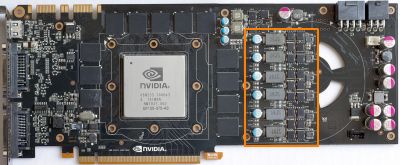
GTX 480 PCB front
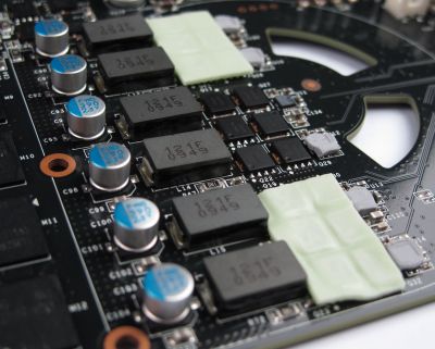
GTX 480 GPU VRM phases details (source)
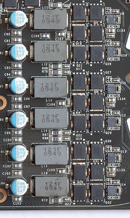
GTX 480 GPU VRM phases details
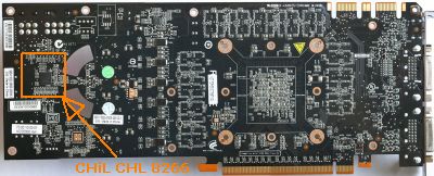
GTX 480 PCB back with the voltage controller
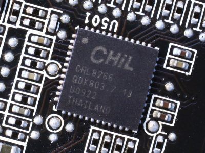
GTX 480 voltage controller detail (source)
Each phase of the GTX 480 GPU VRM is made up of three MOSFETs, one choke and one capacitor.
References and useful links
- MOSFET @ wikipedia
- Power MOSFET @ wikipedia
- PWM @ wikipedia
- Pulse Width Modulation @ acroname.com
- Electronic filter @ wikipedia
- Digital techniques for power modules
- Microprocessor Power Management
- Voltage Controlled PWM Generator
- High Current Inductors
- Chokes Explained
- Nvidia GeForce GTX 480 1,536MB Review
- Voltage Regulator on the GTX 480/470
- Radeon HD 5870 Power Circuit @ xbitlabs.com
- Radeon HD 4890 PCB Design @ xbitlabs.com
- ATI Radeon HD 2900 XT – A Closer Look @ techpowerup.com
Pingback: GeForce GTX 275 VRM Damaged by FurMark - 3D Tech News, Pixel Hacking, Data Visualization and 3D Programming - Geeks3D.com
Pingback: Thermalright Spitfire VGA cooler and VRM-R5 Heatsinks Tested With FurMark - 3D Tech News, Pixel Hacking, Data Visualization and 3D Programming - Geeks3D.com
Pingback: Thermalright Does Not Like FurMark… - 3D Tech News, Pixel Hacking, Data Visualization and 3D Programming - Geeks3D.com
Pingback: GTX 480 Cooled by Gelid ICY VISION and Stressed by Kombustor - 3D Tech News, Pixel Hacking, Data Visualization and 3D Programming - Geeks3D.com
Pingback: Nvidia GTX 460 Discussion - Page 3 - Digit Technology Discussion Forum - Tech Discussion Forums in India
Pingback: MSI N460GTX Hawk Designed for Massive Overclocking - 3D Tech News, Pixel Hacking, Data Visualization and 3D Programming - Geeks3D.com
Pingback: Tutorial Mengenai VRM (Voltage Regulator Modules) Pada VGA - Hardware Article
Pingback: MSI GTX 480 Lightning: 16-Phase VRM and 3 Power Connectors - 3D Tech News, Pixel Hacking, Data Visualization and 3D Programming - Geeks3D.com
Pingback: Confused with MOSFETS and VRMs - Page 2 - Overclock.net - Overclocking.net
Pingback: [Tested] ASUS ENGTX580 1536MB at Geeks3D Labs - 3D Tech News, Pixel Hacking, Data Visualization and 3D Programming - Geeks3D.com
Pingback: [Tested] SAPPHIRE Radeon HD 6870 1024MB Review - 3D Tech News, Pixel Hacking, Data Visualization and 3D Programming - Geeks3D.com
Pingback: [Tested and Burned] EVGA GeForce GTX 580 SC Review - 3D Tech News, Pixel Hacking, Data Visualization and 3D Programming - Geeks3D.com
Pingback: A short Power Phase Design explanation - Overclock.net - Overclocking.net
Pingback: What 460? - Page 2 - Overclock.net - Overclocking.net
Pingback: [Tested and Burned] ASUS GeForce GTX 560 Ti DirectCU II TOP Review - 3D Tech News, Pixel Hacking, Data Visualization and 3D Programming - Geeks3D.com