ASUS GeForce GTX 560 DC2 TOP review index
- Page 1 – ASUS GTX 560 DC2 TOP: Presentation
- Page 2 – ASUS GTX 560 DC2 TOP: Features
- Page 3 – ASUS GTX 560 DC2 TOP: OpenGL Tests
- Page 4 – ASUS GTX 560 DC2 TOP: Direct3D Tests
- Page 5 – ASUS GTX 560 DC2 TOP: Gaming Tests
- Page 6 – ASUS GTX 560 DC2 TOP: Power Consumption and Overclocking
- Page 7 – ASUS GTX 560 DC2 TOP: Conclusion
1 – ASUS GeForce GTX 560: Overview
![]()
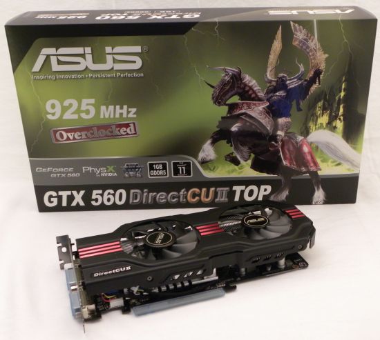
When this card is arrived at Geeks3D lab, I first believed that ASUS made a mistake by sending me again the GTX 560 Ti. But when I started GPU Caps Viewer on this card, the GPU was unknown… I realized this GTX was a new model, a Ti-less model.
NVIDIA new GeForce GTX 560 is priced at USD $199 while you have to add around $20 to get ASUS GTX 560 DC2 TOP. First thing, this GTX 560 like its big brother, the GTX 560 Ti, is designed for massive overclocking. A simple proof: the version sent by ASUS comes with a factory-overclocked GPU at 925MHz… when the reference clock is 810MHz. Another cool thing: we’ll see many customized cards (VGA cooler, PCB) among manufacturers.
In the performance side, this Ti-less GTX 560 is behind the GTX 560 Ti, ahead of the GTX 460 and competes with AMD Radeon HD 6870 and even the HD 6950 in some situations.
That said, let’s quickly talk about the specifications. The GTX 560 is based on the GF114 (like the GTX 560 Ti) clocked at 810MHz (NVIDIA reference clock speed) or at 925MHz in the case of ASUS ENGTX560 DCII TOP. This version of the GF114 packs 336 shader processors. Compared to the GTX 560 Ti, that means that 48 shader processors (or CUDA cores) have been disabled. And 48 CUDA cores form a SM (Streaming Multiprocessor or compute unit in OpenCL world). The GTX 560 has then 7 SM (you can verify this value on the GPU Caps Viewer screenshot related to CUDA, in the next page). And 7 is also the number of SMs in a GTX 460.
The GTX 560 embarks 1024MB of GDDR5 memory (memory interface: 256-bit) clocked at 1002MHz real speed / 4008MHz effective data rate speed (NVIDIA reference clock) or overclocked at 1050MHz real speed(ASUS GTX560 DC2 TOP).
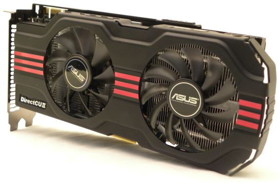
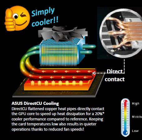
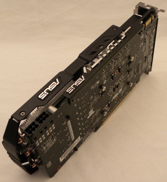
ASUS GTX 560 DC2 TOP is available with the same customized VGA cooler than the GTX 560 Ti. The cooling system, the DirectCU II or DCII, features 2 fans and three copper heatpipes directly in contact with the GPU core:
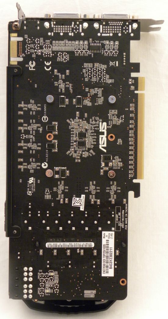
The VGA cooler is customized but also the PCB with its nice black color:
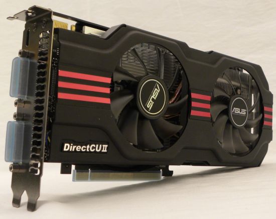
The TDP (or thermal desing power) of NVIDIA GTX 560 reference board is 150W. And the TDP of ASUS GTX 560 DC2 TOP is around 160W (because of the factory overclocking). Two 6-pin power connectors are present on the PCB to meet the power requirement of the whole board:
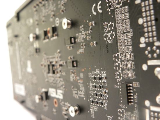
Like the GTX 560 Ti, this GTX 560 has two LEDs on the back side of the PCB, near the power connectors, that show if the card is properly fed or not: green: ok, red: there’s a problem. Here are both LEDs with only one power connector:
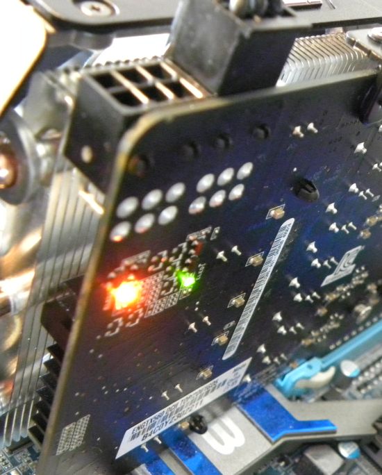
I like this kind of visualization tool!
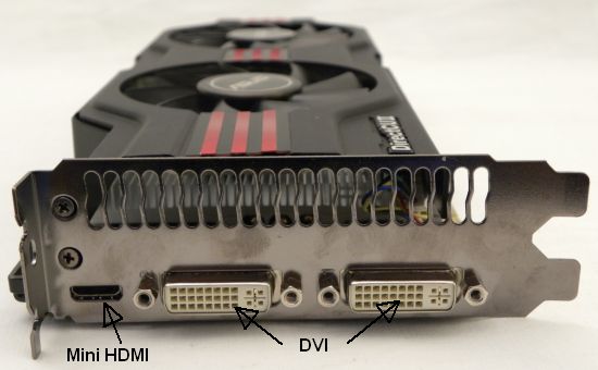
The board features two DVI and one HDMI output connectors:
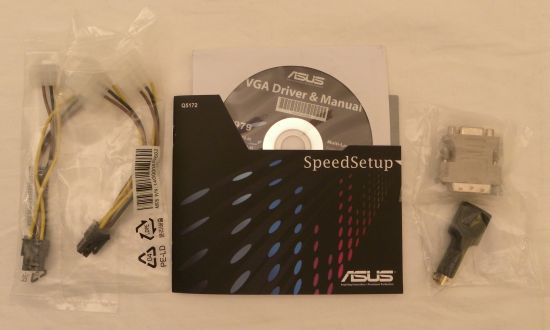
ASUS GTX 560 DC2 TOP bundle includes the box, the card, one mini HDMI-to HDMI adaptor, one DVI-to-D-sub adaptor, two power cables and a CD with drivers (R270.48) and utilities (ASUS Smart Doctor).
ASUS GeForce GTX 560 DC2 TOP review index
- Page 1 – ASUS GTX 560 DC2 TOP: Presentation
- Page 2 – ASUS GTX 560 DC2 TOP: Features
- Page 3 – ASUS GTX 560 DC2 TOP: OpenGL Tests
- Page 4 – ASUS GTX 560 DC2 TOP: Direct3D Tests
- Page 5 – ASUS GTX 560 DC2 TOP: Gaming Tests
- Page 6 – ASUS GTX 560 DC2 TOP: Power Consumption and Overclocking
- Page 7 – ASUS GTX 560 DC2 TOP: Conclusion